What Is Through Silicon Via (TSV) and Its Uses?
TL;DR
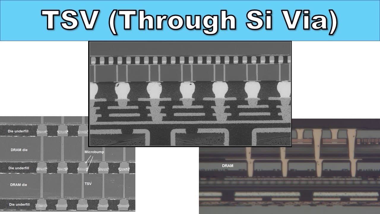
Through Silicon Via (TSV) is a vertical electrical connection in semiconductor packaging that allows for thinner designs, multiple die stacking, and higher data processing capabilities compared to traditional methods like wire bonding. It is utilized in various applications including image sensors, high bandwidth memory (HBM), and silicon interposers. The TSV fabrication process includes techniques such as the Bosch process, enhancing performance in high-speed computing devices.
Transcript
In previous episode, we talked about 2.5D and there was TSV. Today let’s talk about TSV. What is TSV? TSV stands for Through Silicon Via. It is a vertical electrical connection using via and this via go through silicon wafer or die so it is through silicon via. Typically it is made by foundry such as TSMC, UMC, and GlobalFoundry. TSV is an alternat... Read More
Key Insights
- TSV, or Through Silicon Via, is a vertical electrical connection through silicon wafers, providing an alternative to wire bonding and flipchip bonding technology.
- There are three types of TSV: Via first, Via middle, and Via last, each differing in the process flow of fabrication in relation to FEOL and BEOL.
- TSV technology enables the creation of thinner packages and allows for multiple die stacking, offering advantages over traditional technologies like wire bonding and flipchip.
- TSV provides shorter electrical paths, reducing signal delay and power consumption, and offers higher interconnection density for increased data processing capabilities.
- The Bosch process, involving steps like photoresist patterning and isotropic etching, is used to create TSVs, utilizing materials like SF6 gas and C4F8 for etching and passivation.
- TSV structures typically consist of an insulation layer, barrier layer, and are filled with copper, although some remain empty.
- TSV is widely used in applications such as image sensors, high bandwidth memory (HBM), silicon interposers in 2.5D, MEMS, and logic circuits, although the latter is less common due to fabrication challenges.
- The technology is crucial for high-performance computing, allowing for faster data processing and improved video quality in devices like Sony's 3-die stack image sensors.
Install to Summarize YouTube Videos and Get Transcripts
Explore YouTube Video Summarizer or Get YouTube Transcript Extractor
Questions & Answers
Q: What is TSV and why is it important?
TSV, or Through Silicon Via, is a vertical electrical connection through silicon wafers. It is important because it offers an efficient alternative to traditional interconnection techniques like wire bonding and flipchip bonding. TSV enables thinner packages, supports multiple die stacking, and provides shorter electrical paths, leading to reduced signal delay and power consumption.
Q: What are the different types of TSV fabrication processes?
There are three types of TSV fabrication processes: Via first, Via middle, and Via last. 'Via first' involves TSV fabrication before the Front End of Line (FEOL), 'Via middle' occurs between FEOL and Back End of Line (BEOL), and 'Via last' is done after BEOL. Each type has a distinct process flow affecting the final product.
Q: How does the Bosch process contribute to TSV fabrication?
The Bosch process is crucial in TSV fabrication, involving multiple steps like photoresist patterning, isotropic etching, and passivation. It uses materials such as SF6 gas for etching and C4F8 for passivation to create deep, precise TSVs. This process allows for the effective creation of vertical electrical connections in silicon wafers.
Q: What are the advantages of using TSV over traditional technologies?
TSV offers several advantages over traditional technologies like wire bonding and flipchip. It enables the creation of thinner packages without wire loops, supports multiple die stacking, provides shorter electrical paths for reduced signal delay, and consumes less power. Additionally, TSV offers higher interconnection density, allowing for more efficient data processing.
Q: In what applications is TSV technology commonly used?
TSV technology is commonly used in applications such as image sensors, high bandwidth memory (HBM), silicon interposers in 2.5D, MEMS, and logic circuits. It is particularly beneficial in high-performance computing, enhancing data processing speed and video quality, as demonstrated in devices like Sony's TSV-based image sensors.
Q: What materials are typically used in TSV structures?
TSV structures typically consist of an insulation layer, often made of SiO2, and a barrier layer, which may use materials like SiN. The TSV is usually filled with copper (Cu) for electrical conduction, although some TSVs remain empty. These materials are chosen for their compatibility and effectiveness in creating reliable electrical connections.
Q: How does TSV technology impact high-performance computing?
TSV technology significantly impacts high-performance computing by enabling faster data processing and improved video quality. It allows for higher interconnection density, shorter electrical paths, and reduced power consumption, making it ideal for applications requiring rapid data transfer and high efficiency, such as advanced image sensors and memory modules.
Q: What challenges exist in the application of TSV in logic circuits?
The application of TSV in logic circuits presents challenges primarily due to the complexity of fabrication. Creating reliable TSVs in logic circuits requires precise control over the fabrication process, including etching and material deposition. These challenges make TSV less popular in logic applications compared to other uses like image sensors and memory.
Summary & Key Takeaways
-
TSV, or Through Silicon Via, is a technology used in semiconductor packaging that offers an alternative to traditional wire bonding and flipchip bonding. It provides advantages such as thinner packages, multiple die stacking, shorter electrical paths, reduced power consumption, and higher interconnection density.
-
The TSV fabrication process can be categorized into three types: Via first, Via middle, and Via last, based on the sequence of fabrication in relation to FEOL and BEOL stages. The Bosch process, involving steps like photoresist patterning and isotropic etching, is commonly used in TSV creation.
-
TSV technology is applied in various fields, including image sensors, high bandwidth memory, silicon interposers, MEMS, and logic circuits. It is particularly beneficial for high-performance computing, enhancing data processing speed and video quality, as seen in Sony's TSV-based image sensors.
Read in Other Languages (beta)
Share This Summary 📚
Summarize YouTube Videos and Get Video Transcripts with 1-Click
Try YouTube Summary with ChatGPT & Claude or YouTube Transcript Generator
Explore More Summaries from Semicon Talk 📚



Summarize YouTube Videos and Get Video Transcripts with 1-Click
Try YouTube Summary with ChatGPT & Claude or YouTube Transcript Generator