What Is the Flipchip Substrate Manufacturing Process?
TL;DR
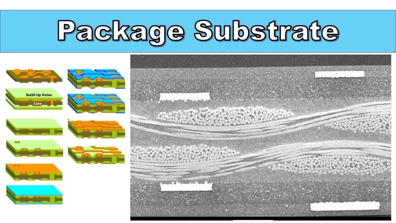
The flipchip substrate manufacturing process involves multiple steps, starting with core-board preparation and ending with flash etching and annealing. Key materials include Ajinomoto Build-up Film (ABF), which is essential for creating complex designs with high I/O capabilities, and both electroless and electrolytic copper plating that establish critical electrical connections.
Transcript
One of my subscribers asked about flipchip package substrate and I decided to make episode for that. So let’s talk about it. Flipchip package substrate looks like this and I will explain about the structure through its manufacturing process and material. One big difference between flipchp package substrate and wirebond package substrate is flipchp ... Read More
Key Insights
- Flipchip package substrates have more I/Os and a complex structure compared to wirebond package substrates, making them suitable for advanced applications.
- The manufacturing process begins with preparing core-boards, which are copper clad laminates consisting of a dielectric with copper foil bonded to both sides.
- Ajinomoto Build-up Film (ABF) is the most popular build-up material used in FCBGA substrates, highlighting its importance in substrate manufacturing.
- Via formation through CO2 laser or UV-YAG laser allows for smaller, more complex designs, essential for the intricate requirements of FCBGA substrates.
- Desmear and electroless copper plating are critical steps to ensure proper electrical connections by removing debris and depositing copper layers.
- Dry film lamination and patterning are used to create masks for copper patterning, which are crucial for establishing electrical signal paths.
- Electrolytic copper plating differs from electroless plating by using electrodes, allowing for faster deposition rates and thicker copper layers.
- The process concludes with flash etching and annealing, finalizing the substrate circuit and completing the manufacturing process.
Install to Summarize YouTube Videos and Get Transcripts
Explore YouTube Video Summarizer or Get YouTube Transcript Extractor
Questions & Answers
Q: What is the main difference between flipchip and wirebond package substrates?
The main difference between flipchip and wirebond package substrates is that flipchip substrates have more input/output (I/O) connections and a more complex structure. This complexity allows flipchip substrates to support advanced applications that require high-density connections, making them more suitable for modern semiconductor technologies.
Q: What role does the core-board play in the manufacturing process?
The core-board, also known as copper clad laminate, serves as the foundational layer in the substrate manufacturing process. It consists of a dielectric material with copper foil bonded to both sides, providing the necessary rigidity and electrical properties required for further processing. This layer is essential for supporting subsequent build-up and plating processes.
Q: Why is Ajinomoto Build-up Film (ABF) significant in substrate manufacturing?
Ajinomoto Build-up Film (ABF) is significant in substrate manufacturing because it is the most popular build-up material used for FCBGA substrates. Its properties make it ideal for creating multilayer structures, allowing for the integration of complex circuit designs. ABF's reliability and performance are crucial for meeting the demands of advanced semiconductor applications.
Q: How are vias formed in the substrate, and why is this important?
Vias are formed using CO2 or UV-YAG lasers, which allow for precise and small hole creation in the substrate. This process is important because vias enable vertical connections between copper layers, facilitating complex circuit designs necessary for high-performance applications. Laser drilling offers advantages over mechanical methods by producing smaller and more intricate vias.
Q: What is the purpose of the desmear and electroless copper plating steps?
The desmear step removes resin and debris from drilling, ensuring a clean surface for copper plating. Electroless copper plating then deposits a uniform copper layer on the substrate without using electrodes. These steps are crucial for establishing reliable electrical connections between layers, which is essential for the functionality of the substrate.
Q: How does dry film lamination contribute to the manufacturing process?
Dry film lamination contributes to the manufacturing process by providing a mask used for creating copper patterns. This film is laminated onto the substrate and then patterned through lithography, allowing for precise control over the electrical signal paths. The accuracy of this step is vital for ensuring the substrate meets design specifications.
Q: What distinguishes electrolytic copper plating from electroless plating?
Electrolytic copper plating differs from electroless plating in that it uses electrodes to deposit copper, allowing for faster deposition rates and thicker layers. While electroless plating can deposit copper on insulators, electrolytic plating is restricted to conductive surfaces. This distinction is important for achieving desired layer thickness and deposition speed.
Q: What are the final steps in the substrate manufacturing process?
The final steps in the substrate manufacturing process include flash etching and annealing. Flash etching removes unnecessary metal layers, refining the substrate circuit. Annealing, or full curing, completes the manufacturing process, ensuring all materials are properly bonded and the substrate is ready for use. These steps finalize the substrate's electrical and structural integrity.
Summary & Key Takeaways
-
The flipchip substrate manufacturing process involves several steps, starting with core-board preparation and ending with flash etching and annealing. This process is essential for creating substrates with complex designs and high I/O capabilities, crucial for advanced semiconductor applications.
-
Ajinomoto Build-up Film (ABF) plays a significant role in substrate manufacturing, providing a reliable build-up material for FCBGA substrates. The use of lasers for via formation allows for intricate designs, meeting the demands of modern technology.
-
Copper plating, both electroless and electrolytic, is vital for establishing electrical connections across substrate layers. The manufacturing process emphasizes precision and detail, ensuring substrates meet the high standards required for semiconductor packaging.
Read in Other Languages (beta)
Share This Summary 📚
Summarize YouTube Videos and Get Video Transcripts with 1-Click
Try YouTube Summary with ChatGPT & Claude or YouTube Transcript Generator
Explore More Summaries from Semicon Talk 📚
![[Eng Sub] Wafer Backgrinding Process: Wafer thinning, Wafer lapping thumbnail](/_next/image?url=https%3A%2F%2Fi.ytimg.com%2Fvi%2Fo1sJnATu7ds%2Fhqdefault.jpg&w=750&q=75)
![[Eng Sub] Laser Dicing - Ablation thumbnail](/_next/image?url=https%3A%2F%2Fi.ytimg.com%2Fvi%2FuDTMJksf5W8%2Fhqdefault.jpg&w=750&q=75)
Summarize YouTube Videos and Get Video Transcripts with 1-Click
Try YouTube Summary with ChatGPT & Claude or YouTube Transcript Generator