[Eng Sub] Wafer Backgrinding Process: Wafer thinning, Wafer lapping
TL;DR
Wafer backgrinding thins wafers for slim electronics.
Transcript
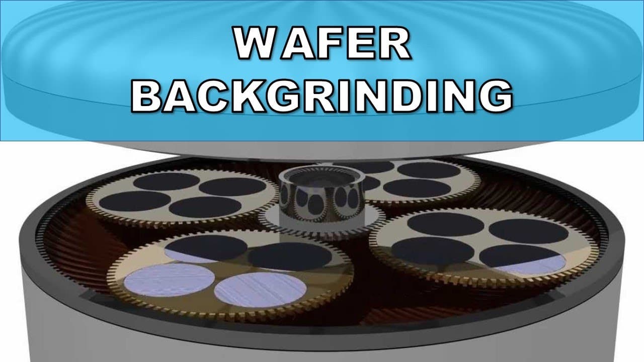
Today I’d like to talk about wafer backgrinding process. This is the first step of semiconductor packaging process. Before we talk about this, let’s think little about wafer first, which is used in wafer backgrinding process. Semiconductor wafer is a thin circle-shape plate typically made of silicon and has integrated circuit on top. But on bac... Read More
Key Insights
- Wafer backgrinding is the initial step in semiconductor packaging, crucial for reducing wafer thickness to fit slim electronics like smartphones.
- Silicon wafers are circular due to the manufacturing process that ensures purity, essential for precise electrical signal control in semiconductors.
- Silicon is favored for semiconductors due to its excellent electrical and mechanical properties and its abundance, making it cost-effective.
- The backgrinding process involves two main steps: grinding to remove most of the wafer thickness and polishing to eliminate surface damage.
- Typical wafer dimensions before backgrinding are 300mm in diameter and 775um in thickness, with weights around 125g.
- Post-backgrinding thickness varies by device type: logic devices to 100um, DRAM to 50um, and NAND to 30um.
- The circular shape of silicon wafers is optimal for achieving high purity, which is critical for semiconductor functionality.
- Wafer backgrinding, also known as wafer thinning or lapping, is essential for reducing semiconductor package height.
Install to Summarize YouTube Videos and Get Transcripts
Explore YouTube Video Summarizer or Get YouTube Transcript Extractor
Questions & Answers
Q: Why is the wafer backgrinding process important?
The wafer backgrinding process is important because it reduces the thickness of silicon wafers, enabling the production of slimmer electronic devices. This process is crucial for meeting the demands of modern electronics, such as smartphones, which require compact and lightweight components without compromising functionality.
Q: Why are silicon wafers circular?
Silicon wafers are circular because the manufacturing process that ensures high purity naturally results in a circular shape. The circular form is optimal for achieving the desired purity level, which is essential for precise electrical signal control in semiconductor applications, making it the preferred shape over squares or rectangles.
Q: What are the typical dimensions of a silicon wafer before backgrinding?
Before backgrinding, a typical silicon wafer measures 300mm in diameter and 775um in thickness. The wafer weighs approximately 125 grams. These dimensions are standard for wafers used in semiconductor manufacturing, providing a starting point for the backgrinding process, which reduces thickness for specific device requirements.
Q: How does the backgrinding process affect wafer thickness?
The backgrinding process significantly reduces wafer thickness to meet the specific requirements of different electronic devices. For example, logic devices are reduced to around 100um, DRAM memory devices to about 50um, and NAND memory devices to approximately 30um. This thickness reduction is crucial for fitting components into slim electronic products.
Q: What are the two main steps in the wafer backgrinding process?
The two main steps in the wafer backgrinding process are grinding and polishing. Grinding involves using a rotating grinding wheel to remove most of the silicon wafer's thickness. Polishing follows, using a polishing wheel to eliminate any mechanical damage caused by grinding, resulting in a smooth, thinned wafer surface.
Q: Why is silicon the preferred material for semiconductors?
Silicon is the preferred material for semiconductors due to its excellent electrical and mechanical properties, which are ideal for semiconductor applications. Additionally, silicon is the most abundant element in the Earth's crust, making it a cost-effective option. Its properties and availability make it the optimal choice for semiconductor manufacturing.
Q: What is the significance of wafer thickness in semiconductor packaging?
Wafer thickness is significant in semiconductor packaging because it determines the overall height of the semiconductor package. Reducing wafer thickness through backgrinding allows for the creation of slimmer packages, essential for modern, compact electronic devices like smartphones, where space and weight are critical considerations for design and functionality.
Q: What challenges does the backgrinding process address in semiconductor manufacturing?
The backgrinding process addresses the challenge of reducing wafer thickness to meet the demands of modern electronic devices, which require compact and lightweight components. By thinning the wafers, manufacturers can produce slimmer semiconductor packages, crucial for integrating into space-constrained applications such as smartphones and other portable devices.
Summary & Key Takeaways
-
Wafer backgrinding is a crucial process in semiconductor packaging, aimed at reducing wafer thickness to meet the demands of slim electronic products. The process starts with grinding to remove most of the wafer thickness and is followed by polishing to eliminate surface damage.
-
Silicon wafers are circular to ensure purity, which is vital for precise electrical signal control in semiconductors. Silicon's abundance and properties make it the preferred material for semiconductors, offering a cost-effective solution with excellent electrical and mechanical characteristics.
-
The wafer backgrinding process involves placing the wafer on a rotary table with its backside facing upward. The grinding wheel removes most of the thickness, and the polishing wheel smooths the surface, resulting in a thinned wafer suitable for slim electronic devices.
Read in Other Languages (beta)
Share This Summary 📚
Summarize YouTube Videos and Get Video Transcripts with 1-Click
Try YouTube Summary with ChatGPT & Claude or YouTube Transcript Generator
Explore More Summaries from Semicon Talk 📚
Summarize YouTube Videos and Get Video Transcripts with 1-Click
Try YouTube Summary with ChatGPT & Claude or YouTube Transcript Generator