What Is Transfer Molding and How Does It Work?
TL;DR
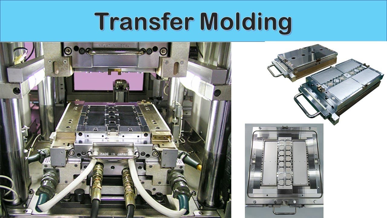
Transfer molding is a semiconductor packaging process that fills mold cavities with a molten molding compound to protect dies and wires. Key steps include heating the mold, loading the substrate, clamping, transferring the compound, and curing. This method is vital for producing various package types and requires precise temperature control to avoid defects like mold flash and voids.
Transcript
Hello everyone, welcome to Semicon Talk. Today let’s talk about transfer molding. Molding is a semiconductor packaging process to protect die and wires from environment. It covers dies and wires by filling mold compound and there are many different methods. Among them transfer molding and compression molding are 2 major methods. Transfer Mol... Read More
Key Insights
- Transfer molding is a prevalent method in semiconductor packaging, primarily used for wirebonding, flipchip, leadframe, and laminate packages.
- The process involves heating the mold to ensure the molten molding compound fills the cavity efficiently, typically requiring a uniform temperature of 175℃.
- Key steps in transfer molding include substrate loading, molding compound preheating, mold clamping, transfer of molten compound, and curing to solidify the compound.
- Mold clamping is crucial to prevent defects such as mold flash, which occurs when excess compound spreads outside the package.
- Post Mold Cure (PMC) is essential to stabilize the molding compound chemically, completing the curing process started during molding.
- Common defects in molding include incomplete molds, mold flash, voids, contamination, scratches, chip offs, and wire sweeps, which can impact the package quality.
- The mold chase, a critical component in the process, requires precise manufacturing, abrasion resistance, and good releasability to ensure efficient production.
- Transfer molding uses pellet-type solid-state molding compounds, and cleaning the mold chase involves melamine compounds to maintain process integrity.
Install to Summarize YouTube Videos and Get Transcripts
Explore YouTube Video Summarizer or Get YouTube Transcript Extractor
Questions & Answers
Q: What is the primary purpose of transfer molding in semiconductor packaging?
Transfer molding is used to protect semiconductor dies and wires by encapsulating them in a mold compound. This process prevents environmental damage and ensures the structural integrity of the semiconductor package. It is an essential step in the manufacturing of various package types, including wirebonding and flipchip packages.
Q: Why is it important to heat the mold before starting the transfer molding process?
Heating the mold is crucial to ensure the molten molding compound flows properly into the mold cavity. If the mold is not preheated, the compound may cool too quickly, slowing its flow and potentially leading to incomplete filling of the cavity. Uniform heating to around 175℃ is typically required for optimal results.
Q: What are some common defects encountered in the transfer molding process?
Common defects in transfer molding include incomplete molds, where parts of the cavity remain unfilled, mold flash, where excess compound spreads outside the package, voids inside the package, contamination from foreign materials, surface scratches, chip offs, and wire sweeps, which can cause wires to bend or disconnect.
Q: How does the mold chase contribute to the transfer molding process?
The mold chase is a critical component that defines the package outline and must be manufactured with precision. It needs to withstand mechanical abrasion during molding and should allow for easy release of the molded package. Special coatings are often applied to enhance its abrasion resistance and releasability.
Q: What role does the Post Mold Cure (PMC) play in the transfer molding process?
The Post Mold Cure (PMC) process completes the curing of the molding compound, ensuring it reaches a chemically stable state. While the initial curing occurs during molding, PMC is necessary to achieve the final solidification and stability of the compound, which is crucial for the durability and reliability of the package.
Q: What is mold flash, and how can it be prevented?
Mold flash is a defect where excess molding compound escapes the intended package boundaries, resulting in unwanted material on the outside of the package. It can be prevented by ensuring proper mold clamping force, which keeps the mold tightly closed and prevents the compound from leaking out during the process.
Q: Why is uniform heating of the mold important in transfer molding?
Uniform heating ensures that the molding compound remains at the right temperature to flow evenly into all parts of the mold cavity. Uneven heating can lead to variations in flow speed, potentially causing incomplete filling or defects like voids. Maintaining a consistent temperature is essential for achieving high-quality results.
Q: How does transfer molding differ from compression molding?
Transfer molding involves filling the mold cavity with a molten compound from an external source, whereas compression molding directly compresses the compound within the mold. Transfer molding is typically used for more complex and delicate package types, as it allows for greater control over the flow and distribution of the compound.
Summary & Key Takeaways
-
Transfer molding is a widely used semiconductor packaging process that protects dies and wires by filling them with a mold compound. The method is common for various package types, including wirebonding and flipchip packages. The process involves several steps, such as heating, clamping, and curing, to ensure effective packaging.
-
Key to the transfer molding process are the precise temperatures and pressures applied to ensure the molding compound fills the cavity without defects. Mold flash, voids, and contamination are common issues that can arise if the process is not carefully controlled. Post Mold Cure (PMC) completes the curing process.
-
The mold chase plays a vital role, requiring precision and durability to withstand mechanical abrasion. Its design and maintenance are crucial for preventing defects and ensuring productivity. Despite its seemingly simple appearance, transfer molding is a complex process requiring careful attention to detail.
Read in Other Languages (beta)
Share This Summary 📚
Summarize YouTube Videos and Get Video Transcripts with 1-Click
Try YouTube Summary with ChatGPT & Claude or YouTube Transcript Generator
Explore More Summaries from Semicon Talk 📚


Summarize YouTube Videos and Get Video Transcripts with 1-Click
Try YouTube Summary with ChatGPT & Claude or YouTube Transcript Generator