How Does an SR Latch Work with NOR Gates?
TL;DR
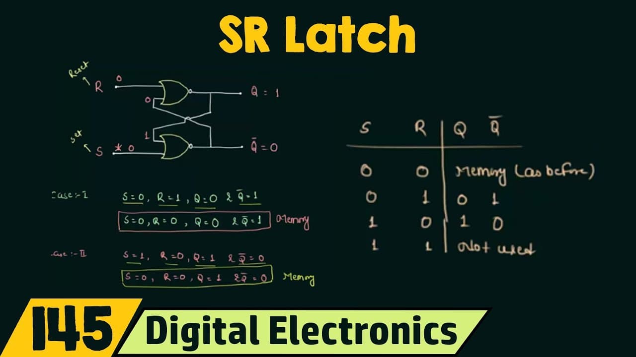
An SR latch is the basic storage element that holds a single bit, built from cross-coupled NOR or NAND gates. With S=0 and R=0 the latch keeps its previous output, so it acts as memory; S=0 R=1 resets Q to 0, and S=1 R=0 sets Q to 1. Setting both S and R to 1 is not used because it forces Q and Q complement to be equal.
Transcript
welcome to lecture number 119 in digital electronics course in the last presentation I explained you basics of sequential circuits and I explained you that the only difference between the combinational circuits and the sequential circuits is the memory block in sequential circuits we have memory element and it is used to store the past output so wh... Read More
Key Insights
- A latch is the basic storage element in sequential circuits, and its purpose is to store a single bit, 0 or 1. Once a single bit can be stored, multi bit numbers such as 100 or 101 can be stored by combining such elements.
- The memory element is what separates sequential circuits from combinational circuits. It stores the past output, and everything else about the two circuit families is otherwise the same according to the presentation.
- The SR latch exists in two forms, the NOR SR latch and the NAND SR latch. Having two forms is treated as a disadvantage, because you must know which gates the internal circuit uses before you can predict its behavior.
- S stands for set and R stands for reset. In digital electronics, set means the output is 1 and reset means the output is 0, so S=1 drives Q to 1 and R=1 drives Q to 0, which is where the input names come from.
- The two input NOR gate truth table drives the whole analysis. The output is 1 only when both inputs are 0, so if any single input is 1, the output is 0 regardless of what the other input is.
- The condition S=0 and R=0 is the memory state. Removing the inputs leaves the outputs unchanged from whatever they were before, and the presentation proves this twice, once after a reset and once after a set.
- The condition S=1 with R=1 makes Q and Q complement both equal to 0, which is a contradiction because the two outputs are defined to always be complements of each other. This is the first reason the combination is not used.
- The second and worse problem with S=1 R=1 appears after the inputs are removed. The resulting output depends on whether Q or Q complement is analyzed first, giving two different valid answers for the same input condition, so the state is unpredictable.
Install to Summarize YouTube Videos and Get Transcripts
Explore YouTube Video Summarizer or Get YouTube Transcript Extractor
Questions & Answers
Q: What is an SR latch in digital electronics?
An SR latch is the basic storage element used in sequential circuits, built to store a single bit of data, either 0 or 1. Its name comes from the way a door latch holds something in place, since the circuit latches a 0 or a 1. It comes in two forms, the NOR SR latch and the NAND SR latch. Once a circuit can store a single bit, multi bit numbers such as 100 or 101 can also be stored. Understanding the latch is described as the most important point in sequential circuits, since flip flops, counters and registers all build on it.
Q: What is the difference between combinational and sequential circuits?
The only difference between combinational circuits and sequential circuits is the memory block present in sequential circuits. Sequential circuits contain a memory element that is used to store the past output, while combinational circuits do not. That memory element is what allows a sequential circuit to retain information about what happened earlier, and the basic version of that memory element is the latch. Everything else about the two circuit families is otherwise the same, so the memory block is the single defining distinction between them.
Q: Why are the SR latch inputs called S and R?
R stands for reset and S stands for set. In digital electronics, saying reset means the output is made equal to 0, and saying set means the output is made equal to 1. So when the S input is equal to 1, it makes the output Q equal to 1, and when the R input is equal to 1, it makes the output Q equal to 0. The naming directly reflects what each input does to the output, and the presentation proves this behavior through gate level analysis using the NOR gate truth table.
Q: How does an SR latch store data when both inputs are 0?
When S=0 and R=0, the latch is in its memory state and holds whatever output it had before. This works because of the cross coupled feedback. If Q complement was 1, that 1 feeds into the other NOR gate along with R=0, giving inputs 0 and 1, whose NOR output is 0, so Q stays 0. That 0 feeds back with S=0 to give inputs 0 and 0, whose NOR output is 1, so Q complement stays 1. The outputs reinforce each other and the stored data is preserved after the inputs are removed.
Q: What is the NOR gate truth table used in SR latch analysis?
The analysis uses a two input NOR gate with inputs A and B and output Y, which has four possible input combinations. The output is 1 when both inputs are 0, and the output is 0 for the other three combinations. The practical shortcut used throughout the analysis is that if any input is 1, the output is going to be 0 and you do not have to look at the other input at all. This rule is what makes the case by case latch analysis quick to follow.
Q: Why is S=1 and R=1 not used in an SR latch?
Setting both S and R to 1 is not used for two reasons. First, R=1 forces Q to 0 and S=1 forces Q complement to 0 at the same time, so Q equals Q complement, which is a contradiction because the two outputs must always be complements of each other. Second, if you then remove the inputs by setting both to 0, the result depends on which output you analyze first. Starting from Q gives Q=0 and Q complement=1, while starting from Q complement gives Q=1 and Q complement=0. The same input condition producing two different outputs makes the state unusable.
Q: What happens when S=0 and R=1 in a NOR SR latch?
When S=0 and R=1, the latch resets. Because any input equal to 1 forces a NOR gate output to 0, the R=1 input makes Q equal to 0, which matches the meaning of reset. That Q value of 0 is fed back to the input of the other NOR gate, which then sees inputs of 0 and 0 from S and from Q, so its output is 1, making Q complement equal to 1. The outputs are complements of each other as required, giving Q=0 and Q complement=1.
Q: Why does an SR latch need a clock?
The latch has a drawback compared with a real door latch. With a door, once latched, nothing inside can get out and nothing outside can get in, but with the SR latch, if the S or R inputs change, the stored data changes with them. Those inputs may change accidentally or intentionally, because the latch is used along with other circuits and S and R may be connected to another circuit's output. If that output changes, the stored data is removed. Adding a clock overcomes this by controlling when the stored data can change.
Summary & Key Takeaways
-
The only difference between combinational and sequential circuits is the memory block, which stores past output. The aim of the basic storage element is to store a single bit, either 0 or 1, and once a single bit can be stored, multi bit numbers such as 100 or 101 can also be stored. That basic storage element is called a latch.
-
The SR latch comes in two types, the NOR SR latch and the NAND SR latch. This is described as a disadvantage, because every time you work with one you need to know the internal circuit and whether NOR or NAND gates are being used. The name latch comes from the way a door latch holds something in place, holding either 0 or 1 in the circuit.
-
Unlike a door latch, the stored data can be changed whenever the S and R inputs change, accidentally or intentionally, because the latch is used together with other circuits and S and R may be driven by another circuit's output. If that output changes, the stored data is removed. This drawback is overcome by adding a clock, which is covered in the following presentation.
-
R stands for reset and S stands for set. In digital electronics, reset means the output is 0 and set means the output is 1. So making R equal to 1 drives Q to 0, and making S equal to 1 drives Q to 1. The analysis uses the two input NOR gate truth table, where the output is 1 only when both inputs are 0.
-
In case one, S=0 and R=0 gives Q=0 and Q complement=1, because R=1 forces Q to 0 and the fed back 0 with R makes Q complement 1. Removing the inputs by setting S=0 and R=0 keeps Q=0 and Q complement=1, proving that the 0,0 input condition holds the previously stored data.
-
In case two, S=1 and R=0 makes Q complement 0, and that 0 fed back with R=0 makes Q equal to 1. Returning the inputs to S=0 and R=0 again preserves Q=1 and Q complement=0. This proves for a second time that the 0,0 input condition is the memory state where previous values are retained.
-
In case three, S=1 and R=1 makes both Q and Q complement 0 at the same time, a contradiction because the two outputs must always be complements of each other. This alone shows the configuration is invalid, but the presentation notes a second and more disturbing problem that appears when the inputs are then removed.
-
After S=1 R=1, setting both inputs back to 0 gives different results depending on which output is analyzed first. Starting the analysis from Q gives Q=0 and Q complement=1, while starting from Q complement gives Q=1 and Q complement=0. Because the same input condition yields two different outputs, S=1 with R=1 is marked not used.
Read in Other Languages (beta)
Share This Summary 📚
Summarize YouTube Videos and Get Video Transcripts with 1-Click
Try YouTube Summary with ChatGPT & Claude or YouTube Transcript Generator
Explore More Summaries from Neso Academy 📚




Summarize YouTube Videos and Get Video Transcripts with 1-Click
Try YouTube Summary with ChatGPT & Claude or YouTube Transcript Generator