[Eng Sub] Intel EMIB
TL;DR
Intel EMIB connects dies with small silicon bridges, offering cost-effective alternatives to 2.5D interposers.
Transcript
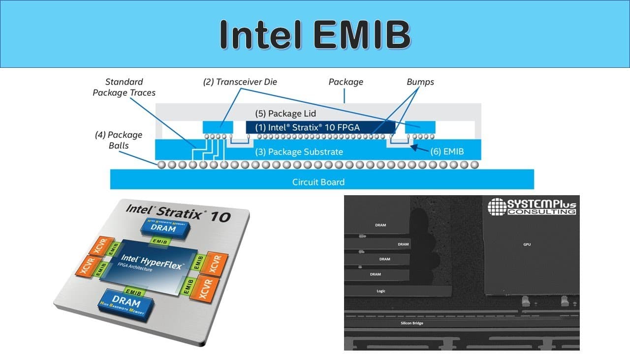
Hello everyone, welcome to Semicon Talk! Today’s topic is Intel EMIB. Let’s talk about it. EMIB stands for Embedded Multi-die Interconnect Bridge. It is technology to connect dies using small silicon bridge and it is developed by Intel. Small silicon bridge looks like this and we can imagine its size by comparing with a rice grain. It will be b... Read More
Key Insights
- EMIB, or Embedded Multi-die Interconnect Bridge, is a technology developed by Intel to connect dies using small silicon bridges, offering a more cost-effective solution compared to traditional 2.5D interposers.
- Unlike 2.5D technology, which uses large silicon interposers limited by reticle size and expensive TSV structures, EMIB employs small silicon bridges that are not constrained by reticle size, reducing manufacturing costs.
- The structure of EMIB technology involves embedding silicon bridges within the package substrate, allowing for electrical connections between dies through vias and traces, enhancing interconnectivity without the need for TSVs.
- EMIB's silicon bridge features two different bump arrays on the dies it connects: a 55um pitch bump array for the silicon bridge area and a 130um pitch bump array for the package substrate area.
- The silicon bridge in EMIB technology can vary in size from 2x2mm to 8x8mm and contains up to four metal layers, facilitating efficient interconnection between dies.
- The EMIB manufacturing process involves several steps, including the preparation of a package substrate with a cavity, precise placement of the silicon bridge, and the use of dielectric films and Cu plating for via formation and connectivity.
- Intel's EMIB technology has been applied in products like the Kaby Lake-G mobile microprocessor, where it connects GPUs and HBM memory modules, and in Intel Agilex FPGA, linking various components like transceivers and Ethernet interfaces.
- EMIB provides a scalable and flexible solution for modern electronic devices, enabling high-density interconnects and efficient data transfer between components, crucial for advanced computing applications.
Install to Summarize YouTube Videos and Get Transcripts
Explore YouTube Video Summarizer or Get YouTube Transcript Extractor
Questions & Answers
Q: What is EMIB technology?
EMIB, or Embedded Multi-die Interconnect Bridge, is a technology developed by Intel to connect multiple dies using small silicon bridges. This approach offers a cost-effective and flexible alternative to traditional 2.5D interposers, eliminating the need for expensive TSV structures and overcoming reticle size limitations.
Q: How does EMIB differ from 2.5D technology?
EMIB differs from 2.5D technology by using small silicon bridges instead of large silicon interposers. This eliminates the need for TSV structures, reducing costs, and is not constrained by reticle size. These differences make EMIB a more flexible and cost-effective solution for die interconnection.
Q: What is the structure of EMIB technology?
The structure of EMIB technology involves embedding silicon bridges within the package substrate. Dies are placed on top of this substrate and are connected electrically through vias and traces, without requiring TSVs. This design allows for efficient interconnectivity between dies using different pitch bump arrays.
Q: What are the key components of EMIB's silicon bridge?
EMIB's silicon bridge features two different bump arrays: a 55um pitch bump array for silicon bridge connections and a 130um pitch bump array for package substrate connections. The bridge itself can vary in size and contains up to four metal layers, facilitating effective inter-die connections.
Q: What is the manufacturing process of EMIB technology?
The EMIB manufacturing process involves preparing a package substrate with a cavity, precisely placing the silicon bridge, and using dielectric films and Cu plating for via formation. This process enables the creation of efficient electrical connections between dies through the embedded silicon bridge.
Q: What are some applications of EMIB technology?
EMIB technology is applied in products like Intel's Kaby Lake-G microprocessor, where it connects GPUs and HBM memory modules, and in the Intel Agilex FPGA, linking components such as transceivers and Ethernet interfaces. These applications highlight EMIB's versatility and effectiveness in advanced computing.
Q: How does EMIB enhance interconnectivity in electronic devices?
EMIB enhances interconnectivity by embedding silicon bridges within package substrates, allowing for efficient electrical connections between dies without the need for TSVs. This design supports high-density interconnects and efficient data transfer, crucial for advanced computing applications.
Q: Why is EMIB considered a cost-effective solution?
EMIB is considered cost-effective because it eliminates the need for expensive TSV structures used in traditional 2.5D interposers. Additionally, its use of small silicon bridges instead of large interposers reduces manufacturing costs and overcomes reticle size limitations, offering a scalable solution for die interconnection.
Summary & Key Takeaways
-
Intel's EMIB technology connects dies using small silicon bridges, offering a cost-effective alternative to 2.5D interposers. It eliminates the need for expensive TSV structures and is not limited by reticle size, making it a flexible solution for modern electronics.
-
The structure of EMIB involves embedding silicon bridges within package substrates, facilitating electrical connections between dies through vias and traces. This design allows for efficient interconnectivity without the constraints of traditional silicon interposers.
-
EMIB technology has practical applications in products like Intel's Kaby Lake-G microprocessor and Agilex FPGA, where it connects GPUs, memory modules, and various interfaces, demonstrating its versatility and effectiveness in advanced computing environments.
Read in Other Languages (beta)
Share This Summary 📚
Summarize YouTube Videos and Get Video Transcripts with 1-Click
Try YouTube Summary with ChatGPT & Claude or YouTube Transcript Generator
Explore More Summaries from Semicon Talk 📚

Summarize YouTube Videos and Get Video Transcripts with 1-Click
Try YouTube Summary with ChatGPT & Claude or YouTube Transcript Generator