How Does China's CHIPX Photonic Quantum AI Chip Claim 1,000× Faster Performance Than NVIDIA?
TL;DR
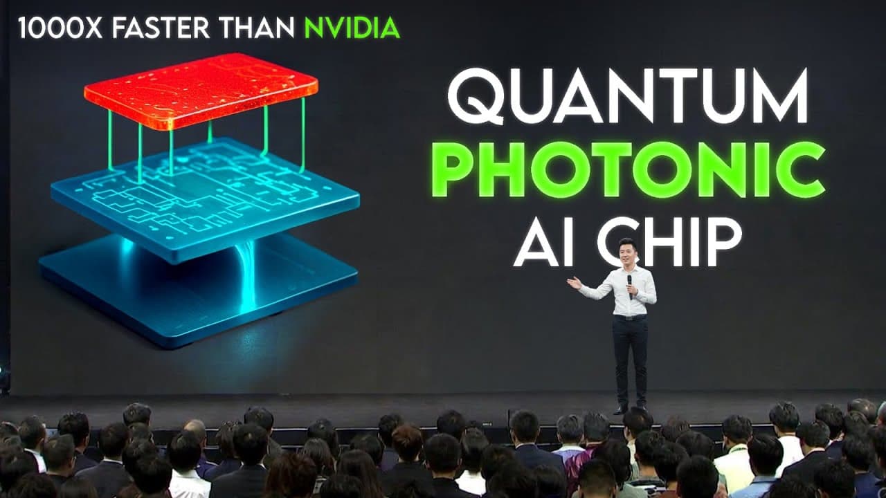
China’s CHIPX photonic quantum AI chip works as a programmable accelerator that processes information through light’s color, timing, phase, and distribution within a quantum-classical hybrid architecture. Built with more than a thousand optical components on a 6-inch thin-film lithium niobate wafer, it reportedly accelerates certain AI workloads by up to 1,000 times over NVIDIA GPUs. Read on to understand the claim, deployment progress, and unresolved limitations.
Transcript
China just dropped something wild into the AI race. And honestly, it's the kind of breakthrough that shifts the energy in the entire industry overnight. You're probably used to hearing about quantum computers locked away in labs, hooked up to giant cooling systems, and costing millions to operate. But this time, the story hits way closer to the wor... Read More
Key Insights
- The reported 1,000-fold performance gain applies only to certain AI and complex problem-solving workloads. The transcript explicitly rejects the idea that the chip is 1,000 times faster at everything, and it notes that the exact benchmark behind the comparison with NVIDIA GPUs remains unclear.
- The chip is a programmable photonic accelerator rather than a universal quantum computer. It uses quantum-classical hybrid logic and processes information through light properties such as color, timing, phase, and distribution, making it suitable for specialized AI and high-speed data-processing workloads.
- The hardware is built on a 6-inch thin-film lithium niobate wafer containing more than a thousand optical components. Its monolithic integration places many functions on one wafer, reducing dependence on separate modules and supporting a smaller, more scalable system design.
- Photonic computation is presented as more energy-efficient because photons generate less heat than electrical signaling. The design is intended to address data-center constraints involving power consumption, thermal management, bandwidth, and the growing computational demands associated with training larger AI models.
- Co-packaging places electronic and photonic components close together on the same wafer. According to the transcript, this shorter travel distance reduces latency and noise, increases bandwidth, lowers error rates, and improves throughput by keeping optical signals from moving across long physical pathways.
- Deployment time is reportedly reduced from 6 months to 2 weeks through the integrated photonic design. This faster assembly and integration cycle could make specialized quantum-classical systems easier to install in existing data centers than large, fragile quantum systems requiring lengthy calibration.
- CHIPX's pilot production line is designed to produce 12,000 wafers per year, with approximately 350 chips obtained from each wafer. Production remains a bottleneck because thin-film lithium niobate is delicate, and both manufacturing yield and consistency across wafers still need improvement.
- Independent verification is necessary before treating the reported results as established performance. The transcript identifies unresolved questions about benchmark definitions, workload scope, failure modes, long-term operation, production consistency, and whether the claimed advantages persist under sustained real-world data-center use.
Install to Summarize YouTube Videos and Get Transcripts
Explore YouTube Video Summarizer or Get YouTube Transcript Extractor
Questions & Answers
Q: How does China’s CHIPX photonic quantum AI chip work?
The chip works as a programmable photonic accelerator, using light rather than relying only on electrical signals to carry and process information. It processes properties including color, timing, phase, and distribution within a quantum-classical hybrid architecture. More than a thousand optical components are integrated on a 6-inch thin-film lithium niobate wafer.
Q: Is the CHIPX photonic quantum chip really 1,000 times faster than NVIDIA GPUs?
The developers claim acceleration of up to 1,000 times over NVIDIA GPUs for specific AI workloads and complex problem-solving tasks. The transcript explicitly says it is not 1,000 times faster at everything. The precise benchmark is not clearly disclosed, so the claim still requires independent verification.
Q: Who developed China’s photonic quantum AI chip?
The chip comes from CHIPX, short for Chip Hub for Integrated Photonics Explorer, working with Turing Quantum. They describe it as a scalable, industrial-grade optical quantum chip designed for high-speed AI and data processing.
Q: What is the CHIPX photonic chip made from?
The chip is built on a 6-inch thin-film lithium niobate wafer containing more than a thousand optical components. Its monolithic design integrates the components on one wafer instead of relying on separate modules. The transcript says thin-film lithium niobate is delicate, making production yield and consistency continuing challenges.
Q: Is the CHIPX chip a universal quantum computer?
No, it is photonic quantum hardware optimized for AI acceleration and high-speed data processing rather than a universal quantum computer. It uses quantum-classical hybrid logic and functions as a specialized programmable photonic accelerator.
Q: Why could photonic chips reduce data-center heat and power consumption?
The chip moves information with light, which the transcript says does not generate heat in the same way as electricity and loses less energy during transmission. Photons also enable smoother, more efficient data movement. These properties target the heat and power constraints affecting AI data centers.
Q: How quickly can CHIPX photonic systems be deployed?
CHIPX says systems that normally require 6 months to assemble can be deployed in just 2 weeks with its photonic design. The shorter timeline addresses a major problem with quantum systems, which can be massive, fragile, and slow to build, calibrate, and integrate.
Q: How many chips can the CHIPX pilot production line produce?
The pilot line can produce 12,000 wafers per year, with around 350 chips yielded from each wafer. Its ecosystem covers chip design, fabrication, packaging, testing, and system-level integration. Production remains a bottleneck because yields need improvement and consistency across wafers is still challenging.
Summary & Key Takeaways
-
CHIPX and Turing Quantum developed a programmable photonic accelerator built on a 6-inch thin-film lithium niobate wafer. The monolithic design integrates more than a thousand optical components and processes information through properties of light, including color, timing, phase, and distribution, while operating within a quantum-classical hybrid architecture.
-
The developers claim the chip delivers up to a 1,000-fold acceleration for certain complex AI workloads, not every computing task. Its photonic pathways are presented as offering high bandwidth, low latency, reduced heat, and lower power consumption. Independent verification is still needed to define the benchmark, operating limits, and reliability.
-
Industrialization is central to the announcement. CHIPX says systems that previously required 6 months to assemble can now be deployed in 2 weeks. Its pilot line can produce 12,000 wafers annually, with roughly 350 chips per wafer, while supporting design, fabrication, packaging, testing, and system integration within one ecosystem.
Read in Other Languages (beta)
Share This Summary 📚
Summarize YouTube Videos and Get Video Transcripts with 1-Click
Try YouTube Summary with ChatGPT & Claude or YouTube Transcript Generator
Explore More Summaries from AI Revolution 📚






Summarize YouTube Videos and Get Video Transcripts with 1-Click
Try YouTube Summary with ChatGPT & Claude or YouTube Transcript Generator