How Does a PISO Shift Register Load and Shift?
TL;DR
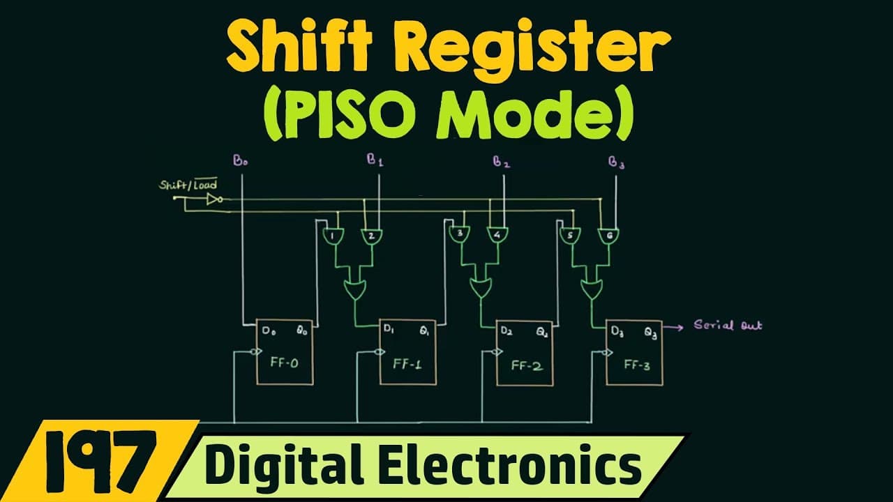
A PISO shift register loads multiple bits simultaneously, then moves them between flip-flops to produce a serial output. An active-low shift/load control selects the operation: zero enables parallel loading of B0 through B3, while one enables shifting from Q0 toward Q3, with the value stored in the final flip-flop appearing at the output.
Transcript
in this lecture I will teach you parallel input serial output mode of shift register it is a very easy and important topic at the same time in this mode the bits are entered in parallel or you can say simultaneously we have four bits B 0 B1 B2 and B3 and we need to enter them in parallel manner one very important thing that you can see in this circ... Read More
Key Insights
- • A PISO shift register is a circuit that accepts several bits simultaneously and then supplies those stored bits through a serial output path.
- • The register has two operating modes: load mode achieves parallel input, while shift mode achieves serial movement and output of the stored data.
- • Load mode is selected when the active-low shift/load complement input is zero, causing the NOT gate to produce one on the load-control path.
- • Parallel loading stores B0 in flip-flop zero, B1 in flip-flop one, B2 in flip-flop two, and B3 in flip-flop three simultaneously.
- • Each interstage combinational circuit uses two AND gates and one OR gate to select either a parallel input bit or the output of the preceding flip-flop.
- • Shift mode is selected by changing the shift/load complement input from zero to one, which enables the interstage Q paths and disables the parallel data paths.
- • Data shifting works by applying Q0 to D1, Q1 to D2, and Q2 to D3, moving each stored value toward the final flip-flop.
- • The serial output is Q3, so the value stored in flip-flop three appears first when shifting begins after the parallel loading operation.
Install to Summarize YouTube Videos and Get Transcripts
Explore YouTube Video Summarizer or Get YouTube Transcript Extractor
Questions & Answers
Q: What is a parallel-input serial-output shift register?
A parallel-input serial-output shift register is a circuit that loads multiple bits at the same time and then moves the stored data toward a single output. In the demonstrated register, B0 through B3 are loaded into four corresponding flip-flops. During shifting, Q0 moves to the second stage, Q1 moves to the third, Q2 moves to the fourth, and Q3 appears as the output.
Q: How does load mode work in a PISO shift register?
Load mode stores all supplied bits simultaneously in their respective flip-flops. B0 is stored in flip-flop zero, B1 in flip-flop one, B2 in flip-flop two, and B3 in flip-flop three. The active-low shift/load complement input is set to zero, enabling the parallel input paths through the combinational circuits and preventing preceding flip-flop outputs from controlling the next stages.
Q: How does shift mode work in a PISO shift register?
Shift mode begins when the shift/load complement input changes from zero to one. This control setting enables the paths carrying the outputs of preceding flip-flops and disables the parallel input paths. Q0 becomes the input to D1, Q1 becomes the input to D2, and Q2 becomes the input to D3. Meanwhile, the value stored at Q3 is supplied as the serial output.
Q: What does the shift/load complement signal control?
The shift/load complement signal determines whether the register loads data in parallel or shifts previously stored data. It is active low for loading, so a value of zero selects load mode. A NOT gate produces the complementary control needed by the selection circuits. Changing the signal to one selects shift mode, enabling the connections between successive flip-flop outputs and inputs.
Q: Why are AND and OR gates used between the flip-flops?
The AND and OR gates form a combinational selection circuit between successive flip-flops. Each circuit contains two AND gates and one OR gate. Depending on the shift/load complement signal, one AND gate passes the parallel input bit while the other is disabled, or the preceding flip-flop output is passed while the parallel path is disabled. The OR gate delivers the selected value to the next flip-flop.
Q: What happens to B0, B1, B2, and B3 during parallel loading?
During parallel loading, the four bits enter their assigned flip-flops simultaneously. B0 enters flip-flop zero, B1 enters flip-flop one, B2 enters flip-flop two, and B3 enters flip-flop three. With the shift/load complement input at zero, the combinational circuits select the B inputs rather than the Q outputs of preceding stages, completing the parallel-input part of the register operation.
Q: What is the serial output of the demonstrated PISO register?
The serial output is Q3, the output of flip-flop three. After parallel loading, the value stored in that final flip-flop is the first value presented at the output when shifting begins. At the same time, Q2 moves into flip-flop three, Q1 moves into flip-flop two, and Q0 moves into flip-flop one, preparing the following stored values to progress toward the output.
Q: How does the bit pattern 1, 0, 1, 1 move through the register?
For the example pattern, B0 is 1, B1 is 0, B2 is 1, and B3 is 1. Load mode stores those values in flip-flops zero through three, respectively. When shift mode begins, the value in flip-flop three produces an output of 1. The preceding values also move forward: Q2 enters flip-flop three, Q1 enters flip-flop two, and Q0 enters flip-flop one.
Summary & Key Takeaways
-
A parallel-input serial-output shift register performs two separate operations. Load mode stores B0, B1, B2, and B3 simultaneously in flip-flops zero through three. This parallel loading accomplishes the input stage, ensuring that every supplied bit enters its corresponding flip-flop during the same operating mode.
-
The shift/load complement signal selects which inputs reach the flip-flops through combinational circuits containing two AND gates and one OR gate. When the signal is zero, the inverted control becomes one, enabling the parallel data paths while disabling the paths that carry outputs from preceding flip-flops.
-
When the control changes to one, the register enters shift mode. The parallel input paths become disabled, while Q0, Q1, and Q2 become the inputs to the following flip-flops. Data consequently moves toward the final stage, and the value held in Q3 becomes the serial output.
Read in Other Languages (beta)
Share This Summary 📚
Summarize YouTube Videos and Get Video Transcripts with 1-Click
Try YouTube Summary with ChatGPT & Claude or YouTube Transcript Generator
Explore More Summaries from Neso Academy 📚






Summarize YouTube Videos and Get Video Transcripts with 1-Click
Try YouTube Summary with ChatGPT & Claude or YouTube Transcript Generator