How does High NA EUV lithography speed chip production?
TL;DR
High NA EUV lithography improves print resolution by enlarging the lens aperture, enabling fewer masks and faster chip production. The system uses a tin droplet plasma light source and Zeiss mirrors in a vacuum, with High NA delivering higher yields and reduced patterning steps, while keeping costs and complexity high. The technology is central to producing advanced chips for major companies.
Transcript
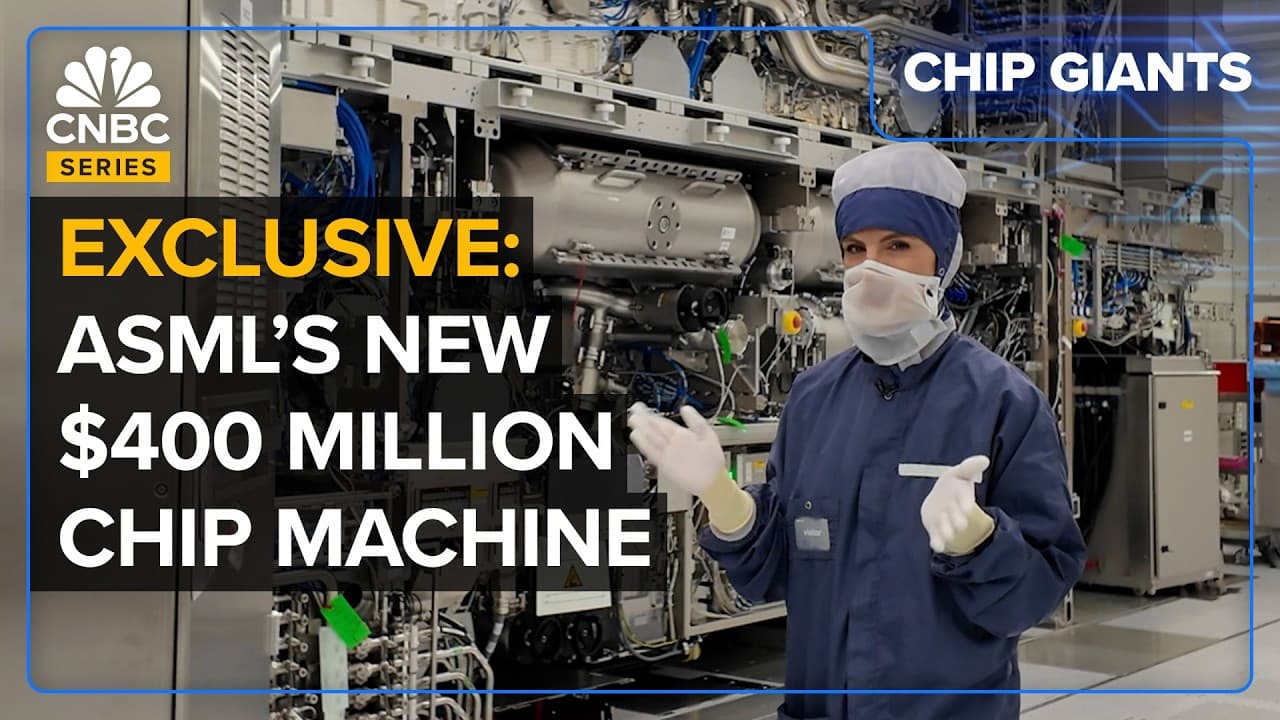
All right. We're about to enter the High NA lab. Behind this highly secured door in an ASML cleanroom. There's a giant $400 million machine. It's bigger than a double-decker bus. Made with such closely protected technical specificity. Very complex. The most advanced machine tool in history. That no filming's ever been allowed, even by ASML's... Read More
Key Insights
- EUV lithography uses light at 13.5 nanometers and requires a vacuum to prevent absorption by materials.
- High NA increases the numerical aperture and enlarges the lens opening to capture more light and resolve smaller features.
- The tiny tin droplets and laser create a plasma that emits EUV light which is captured by a Zeiss collector mirror.
- High NA allows printing in a single exposure, reducing the need for multiple masks compared to older systems.
- ASML has shipped very few High NA machines, reflecting their size, cost, and complexity.
- Maintaining ultra clean conditions in the high NA lab is essential to avoid contamination of precision components.
- Power efficiency improvements have reduced energy per wafer exposure by a substantial margin since EUV began.
- Legacy DUV machines remain in demand and often serve less advanced nodes or markets with export controls in mind.
Install to Summarize YouTube Videos and Get Transcripts
Explore YouTube Video Summarizer or Get YouTube Transcript Extractor
Questions & Answers
Q: A real search query question about the video (e.g. 'How to...', 'What is...', 'Why does...', 'When should...'). Question 1
What is High NA lithography and why does it matter for chip making? High NA lithography refers to a higher numerical aperture in the lithography system that increases the lens opening angle, allowing smaller chip features to be printed in a single exposure. This reduces the number of masks required, speeds up production, and improves yield for advanced logic devices, which is critical for companies like Intel, TSMC and Samsung that rely on ultra fine patterns.
Q: Question 2
How does the EUV light source work in ASML machines? The EUV light is generated by firing four CO2 lasers at tiny tin droplets, causing a plasma that emits photons in the EUV range. Mirrors from Zeiss then direct and focus this light through the projection optics onto the wafer, enabling the printing of nanoscopic chip features in a single exposure under vacuum conditions.
Q: Question 3
Why are High NA machines so expensive and large? High NA machines require bigger mirrors and a more powerful system to capture EUV light at steeper angles. The larger optics and higher power demands translate into higher costs and substantially larger hardware footprints, making only a few machines feasible to produce and ship so far.
Q: Question 4
What role do masks and multiple patterning play in chip fabrication? Traditional lithography uses multiple masks to build up complex patterns in several steps. High NA aims to reduce or even eliminate the need for multiple exposures by enabling smaller features in one pass, which shortens production time and can improve yield for advanced chips.
Q: Question 5
How has power efficiency evolved in EUV systems since their inception? Since EUV began, the energy used per wafer exposure has fallen by more than 60 percent, driven by ongoing improvements in source efficiency, optics, and process control. This trend helps manage overall energy consumption as chip complexity and throughput rise.
Q: Question 6
What challenges surround exporting High NA technology? Export controls and tariffs influence where High NA machines can be deployed. Although some China-bound orders have been restricted, ASML continues to supply other markets, while maintaining safety protocols and compliance with international trade rules, which shapes global semiconductor supply chains.
Q: Question 7
What impact does High NA have on chip production speed and yield? High NA can reduce the number of masks and exposure steps, potentially speeding up fabrication and improving yield by printing more devices per wafer. However, the system’s complexity and risk of lower yield at higher aperture require careful optimization.
Q: Question 8
Where do most chips in everyday devices come from in relation to EUV and DUV? Most chips still rely on legacy DUV lithography for many layers, while EUV-based production is used for the most advanced patterns. DUV machines, though cheaper, remain in strong demand for less demanding nodes and for markets with export restrictions.
Summary & Key Takeaways
-
Summary point 1 describes how EUV lithography uses 13.5 nanometer light and a vacuum system to print chip patterns with photoresist. It highlights the role of mirrors from Zeiss and the need for a controlled environment to avoid contamination.
-
Summary point 2 explains High NA by increasing the lens aperture, allowing single exposure for smaller designs, reducing the number of masks and cutting production time.
-
Summary point 3 notes ongoing challenges such as cost, power use, and complexity, but emphasizes that High NA aims to boost throughput and yield while enabling next generation nodes.
Read in Other Languages (beta)
Share This Summary 📚
Summarize YouTube Videos and Get Video Transcripts with 1-Click
Try YouTube Summary with ChatGPT & Claude or YouTube Transcript Generator
Explore More Summaries from CNBC 📚






Summarize YouTube Videos and Get Video Transcripts with 1-Click
Try YouTube Summary with ChatGPT & Claude or YouTube Transcript Generator