What Are Metal Semiconductor Field-Effect Transistors (MESFETs)? | Microwave Transistors and Tunnel Diodes
TL;DR
Metal semiconductor field-effect transistors (MESFETs) are unipolar microwave devices in which a gate voltage controls majority-carrier flow through a metal–semiconductor junction. They have source, drain, and gate terminals, and can be manufactured using epitaxial growth or ion implantation. Gallium arsenide MESFETs can amplify small signals across the 8–12 GHz X-band while providing low noise and useful power handling, making the operating structure worth exploring further.
Transcript
click the bell icon to get latest videos from ekeeda hello friends i welcome you all to this video we are with chapter 6 of micro engineering where a family of microwave solid-state devices we address along with a start for the microview bipolar junction transistor the physical structure the various configuration of transistor the operating princip... Read More
Key Insights
- 🤘 MESFETs are a type of microwave solid-state device that utilize metal to semiconductor junctions.
- 🤘 Metal to gallium arsenide MESFETs offer higher frequency amplification compared to metal to silicon MESFETs.
- 🔬 MESFETs have three terminals: source, drain, and gate, and their operation is controlled by the voltage applied to the gate terminal.
- 🤌 The pinch-off voltage, which determines the depletion layer width in the semiconductor material, can be calculated using Poisson's equation and boundary conditions.
- 😑 MESFETs can be manufactured using epitaxial or ion implantation processes.
- 🐿️ The dimensions and connections of MESFETs can vary depending on the package or chip device used.
- ⚡ The drain current in MESFETs can be controlled by adjusting the drain voltage.
Install to Summarize YouTube Videos and Get Transcripts
Explore YouTube Video Summarizer or Get YouTube Transcript Extractor
Questions & Answers
Q: What are metal semiconductor field-effect transistors (MESFETs)?
MESFETs are field-effect transistors formed using a metal-to-semiconductor junction. They operate unipolarly with majority charge carriers and belong to the family of microwave solid-state devices.
Q: Why are gallium arsenide MESFETs used for microwave amplification?
A metal-to-gallium-arsenide junction supports higher-frequency operation than the metal-to-silicon alternative described in the transcript. It can amplify small signals across the X-band range of 8 GHz to 12 GHz while offering low noise and the desired power-handling capacity.
Q: What are the three terminals of a MESFET?
A MESFET has source, drain, and gate terminals. The source introduces electrons into the device, the drain removes charge carriers from the semiconductor body, and the gate controls operation through an applied voltage.
Q: How does the gate voltage control a MESFET?
The voltage associated with the gate and drain creates a depletion layer within the epitaxially grown gallium arsenide region. Changing this controlled voltage changes the depletion region and therefore controls carrier flow through the device.
Q: What materials can be used to produce a MESFET?
The transcript identifies metal-to-silicon and metal-to-gallium-arsenide junctions as possible MESFET structures. Gallium arsenide is emphasized because it supports amplification at microwave frequencies.
Q: How can MESFETs be manufactured?
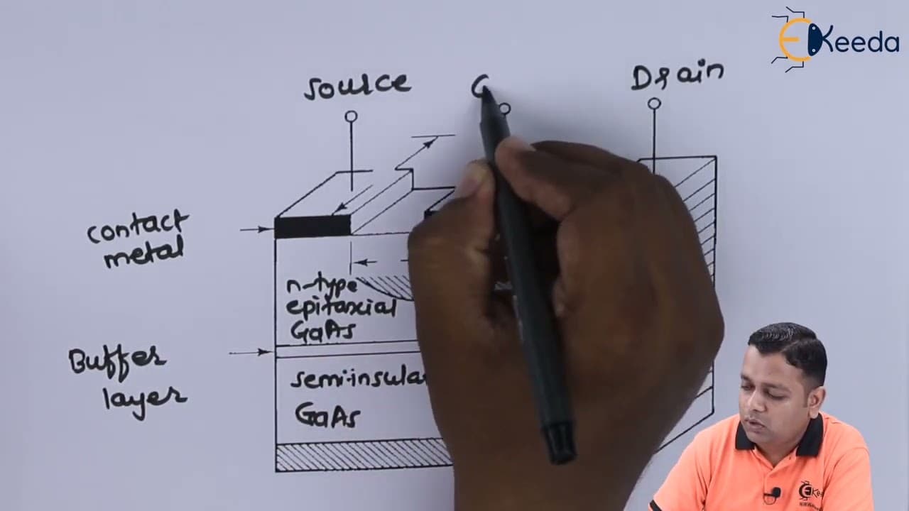
MESFETs can be manufactured using an epitaxial process or ion implantation. In the illustrated structure, an n-type gallium arsenide layer is grown epitaxially above a gallium arsenide buffer layer and a semi-insulating gallium arsenide substrate.
Q: What is the depletion region in an n-channel MESFET?
The depletion region is the shaded area formed inside the semiconductor portion of the device under the controlled gate-to-drain voltage. The transcript associates this region with saturation and the pinch-off voltage condition.
Q: What layers and dimensions appear in the illustrated n-channel MESFET structure?
The structure begins with a semi-insulating gallium arsenide substrate, followed by a gallium arsenide buffer layer and an epitaxially grown n-type gallium arsenide layer connected to metal. The source-to-gate, gate, and gate-to-drain lengths are identified separately, while the vertical dimensions are denoted by small a and capital Z.
Summary & Key Takeaways
-
Metal semiconductor field effect transistors (MESFETs) are a family of microwave transistors that operate with unipolar majority charge carriers.
-
MESFETs can be made using metal to silicon or metal to gallium arsenide junctions, with the latter offering higher frequency amplification up to the microwave range.
-
MESFETs have three terminals: source, drain, and gate, and their operation is controlled by the voltage applied to the gate terminal.
Read in Other Languages (beta)
Share This Summary 📚
Summarize YouTube Videos and Get Video Transcripts with 1-Click
Try YouTube Summary with ChatGPT & Claude or YouTube Transcript Generator
Explore More Summaries from Ekeeda 📚





Summarize YouTube Videos and Get Video Transcripts with 1-Click
Try YouTube Summary with ChatGPT & Claude or YouTube Transcript Generator