SR Latch using NAND gates | Digital Systems Design | Lec-124
TL;DR
The video explains the differences between SR latches made with NAND and NOR gates.
Transcript
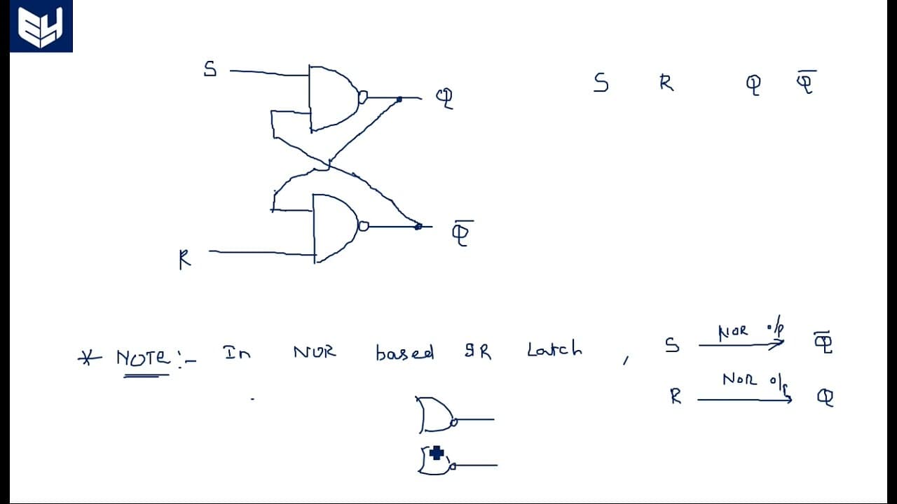
hi everyone in this video I'm going to explain about Sr latch using n gates in the previous video we have seen srl using Nar Gates where the two Nar gates are considered and cross connected with the outputs and the inputs same way we are going to replace the Nar gates with the nand gates but the difference is output and input connections will be di... Read More
Key Insights
- 🇮🇱 SR latches are foundational elements in digital electronics, essential for memory storage.
- 🪈 The connection order of inputs and outputs varies significantly between NAND and NOR latch configurations, affecting circuit behavior.
- 🎨 Invalid states should be carefully managed in both NAND and NOR designs to maintain operational integrity.
- 📡 Transient analysis is crucial for determining circuit performance and reliability during signal changes.
- 🫡 The behavior of NAND latches with respect to reset and set operations is opposite to that of NOR latches.
- ❓ Logical operations in NAND configurations heavily depend on the oscillatory nature of PMOS and NMOS transistors.
- 🌍 Careful consideration of capacitance effects is necessary for accurate transient analysis in real-world applications.
Install to Summarize YouTube Videos and Get Transcripts
Explore YouTube Video Summarizer or Get YouTube Transcript Extractor
Questions & Answers
Q: What is an SR latch and why is it important in digital circuits?
An SR latch is a type of flip-flop used to store a single bit of data. It is fundamental in digital electronics for memory applications and sequential logic circuits. It can maintain its state until explicitly changed, making it crucial for creating stable storage elements in various systems.
Q: How do NAND gates differ from NOR gates when forming SR latches?
In NAND-based SR latches, the outputs directly relate to the same order of inputs, while NOR-based latches involve an inversion of this relation. This leads to different output behavior, specifically in invalid states, which must be carefully considered in design to avoid erroneous outputs.
Q: What does the truth table of the NAND-based SR latch signify?
The truth table indicates the outputs for various input states. For input combinations, if both inputs are zero, the outputs become invalid, while for one input high, the latch responds either by resetting or setting based on the current input states, demonstrating the latch's memory function.
Q: How is the transient analysis of a NAND-based SR latch conducted?
Transient analysis involves adding a lumped capacitance at the output of the circuit, representing internal capacitances of transistors. This capacitance interacts with the required parameters to assess rise and fall times during signal transitions, ensuring accurate computations for circuit performance.
Q: What makes the invalid state in NAND operations different from NOR operations?
In NAND operations, when both inputs are zeros, the output states become invalid, emphasizing that this condition should be avoided. Conversely, for NOR operations, a one-one state is invalid, allowing the previous state to persist until a valid input changes it, highlighting different latch dynamics.
Q: Why does the connection of inputs and outputs matter in NAND-based latches?
The order of inputs and outputs determines the operation of the latch; immediate connections yield specific outputs based on set or reset conditions. Properly maintaining this order is crucial to avoid incorrect output states and ensure reliable circuit behavior.
Q: Can you explain the role of PMOS and NMOS transistors in NAND gates?
In NAND gates, PMOS transistors turn on when inputs are zero, providing a high output, while NMOS transistors conduct when inputs are one. The combination of both types creates the NAND functionality, where only when all inputs are high does the output go low, illustrating how logic levels are managed.
Q: What should be noted when transitioning from NOR to NAND logic in SR latches?
The transition involves changes in how the outputs relate to inputs. Understanding that connections remain in the same order with NAND logic compared to inversed connections with NOR logic is essential to avoid errors in circuit behavior and design implementation.
Summary & Key Takeaways
-
The video focuses on designing an SR latch using NAND gates, contrasting it with NAND latch configurations previously discussed with NOR gates.
-
Key differences are noted in how inputs and outputs are connected, affecting the logical operations, especially when faced with invalid states.
-
The speaker discusses the truth table, output states, and transient analysis, emphasizing the significance of understanding these connections for accurate circuit operation.
Read in Other Languages (beta)
Share This Summary 📚
Summarize YouTube Videos and Get Video Transcripts with 1-Click
Try YouTube Summary with ChatGPT & Claude or YouTube Transcript Generator