How Is an NMOS Transistor Fabricated? | Fabrication Steps | VLSI | Lec-06
TL;DR
NMOS transistor fabrication starts with a P-type substrate and builds the device through oxidation, photolithography, polysilicon deposition, N+ diffusion, insulation, and aluminum metallization. The process forms a 1-micrometer silicon dioxide layer, followed by a thinner 0.1-micrometer oxide layer and two windows for the N+ regions. Read on for the purpose and sequence of each fabrication step.
Transcript
hi everyone in this video I am going to explain what are the different steps involved in the nmos transistor fabrication okay so we will see the step-by-step process and finally we will get the nmos transistor structure the steam the same steps we will also follow in the case of wemos transistor fabrication but the materials will be opposite okay s... Read More
Key Insights
- 🅰️ NMOS transistors require a P-type substrate, contrasting with PMOS, which uses an N-type substrate, highlighting the importance of material selection in semiconductor fabrication.
- 💁 The oxidation process forms a crucial SiO2 layer that protects and insulates different transistor areas during fabrication.
- 👻 Photolithography techniques allow for precise control of which areas undergo further processing, ensuring accurate transistor dimensions and functionality.
- 🪟 The "window structure" created through photolithography is fundamental as it enables targeted diffusion of N+ regions essential for electrical performance.
- 💁 Chemical vapor deposition is a critical method for creating polysilicon layers, which are integral to forming the gate of the NMOS transistor.
- ❓ Effective insulation between semiconductor layers is essential to prevent unintended electrical contacts that could disrupt device operation.
- 🌥️ The metallization step is crucial for connecting the NMOS transistor to external circuits, enabling its integration into larger electronic systems.
Install to Summarize YouTube Videos and Get Transcripts
Explore YouTube Video Summarizer or Get YouTube Transcript Extractor
Questions & Answers
Q: What are the steps involved in NMOS transistor fabrication?
Begin with a P-type substrate, deposit a 1-micrometer silicon dioxide layer through oxidation, and use photolithography and etching to create a window structure. Next, create a 0.1-micrometer oxide layer, deposit polysilicon at the center using chemical vapor deposition, open two windows, and diffuse two N+ regions. The final steps use insulation and aluminum metallization to define the source, gate, and drain terminals.
Q: Why is a P-type substrate used to fabricate an NMOS transistor?
The fabrication process uses the opposite substrate type from the transistor type. Therefore, an NMOS transistor begins with a P-type substrate, while the materials are reversed for PMOS fabrication.
Q: How is the first silicon dioxide layer formed, and how thick is it?
An oxide layer is deposited on the P-type substrate through oxidation. When oxygen reacts with silicon, silicon dioxide forms with a thickness of 1 micrometer.
Q: What is the role of photolithography in NMOS fabrication?
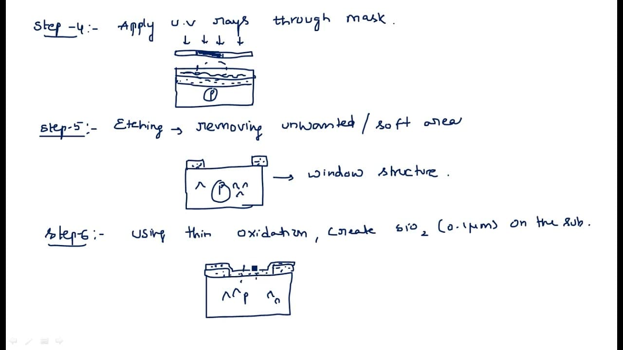
Photolithography selectively removes oxide from areas where later processing must occur. The described sequence applies photoresist, exposes it to UV rays through a mask, and uses etching to remove the unwanted or softened area.
Q: What is the window structure in the NMOS fabrication process?
The window structure has oxide remaining at the ends while the center is open. The open portion provides an area for further fabrication work, while the closed oxide-covered areas provide insulation from nearby devices.
Q: Why is a 0.1-micrometer silicon dioxide layer created after the first window?
After the initial window structure is formed, thin oxidation creates a 0.1-micrometer silicon dioxide layer on the substrate. This oxide is kept at the center while areas on either side are later opened for the two N+ regions.
Q: How is the polysilicon layer created in an NMOS transistor?
Polysilicon is created at the center using chemical vapor deposition. It is placed over the thin oxide layer before photolithography opens the areas on either side for N+ diffusion.
Q: How are the N+ regions and transistor terminals formed?
Photolithography creates two windows on either side of the central polysilicon and oxide structure. Gas is introduced at high temperature during diffusion to form two N+ regions in the P-type substrate. Aluminum metallization and insulation then define the source, gate, and drain terminals.
Summary & Key Takeaways
-
The process of NMOS transistor fabrication involves starting with a P-type substrate, which is essential for creating the necessary electrical properties in NMOS devices.
-
Oxide layers are deposited and selectively removed through photolithography to create a "window structure" crucial for later diffusion and metal deposition processes.
-
The final steps include diffusing N+ regions, metallization with aluminum, and ensuring insulation to define the source, gate, and drain terminals of the transistor.
Read in Other Languages (beta)
Share This Summary 📚
Summarize YouTube Videos and Get Video Transcripts with 1-Click
Try YouTube Summary with ChatGPT & Claude or YouTube Transcript Generator